Monday, June 17, 2013

ATMEGA64

Description

The ATmega64 is a low-power CMOS 8-bit microcontroller based on the AVR enhanced RISC architecture. By executing powerful instructions in a single clock cycle, the ATmega64 achieves throughputs approaching 1 MIPS per MHz, allowing the system designer to optimize power consumption versus processing speed.
The AVR core combines a rich instruction set with 32 general  purpose working registers. All the 32 registers are directly connected to the Arithmetic Logic Unit (ALU), allowing two independent registers to be accessed in one single instruction executed in one clock cycle. The resulting architecture is more code efficient while achieving throughputs up to ten times faster than conventional CISC microcontrollers.

The ATmega64 provides the following features: 64 Kbytes of In-System Programmable Flash with Read-While-Write capabilities, 2 Kbytes EEPROM, 4 Kbytes SRAM, 53 general purpose I/O lines, 32 general purpose working registers, Real Time Counter (RTC), four flexible Timer/Counters with compare modes and PWM, two USARTs, a byte oriented Two-wire Serial Interface, an 8-channel, 10-bit ADC with optional differential input stage with programmable gain, programmable Watchdog Timer with internal  Oscillator, an SPI serial port, IEEE std. 1149.1 compliant JTAG test interface, also used for accessing the On-chip Debug system and programming, and six software selectable power saving modes. The Idle mode stops the CPU while allowing the SRAM, Timer/Counters, SPI port, and interrupt system to continue functioning. The Power-down mode saves the register contents but freezes the Oscillator, disabling all other chip functions until the next interrupt or Hardware Reset. In Power-save mode, the asynchronous timer continues to run, allowing the user to maintain a timer base while the rest of the device is sleeping. The ADC Noise Reduction mode stops the CPU and all I/O modules except asynchronous timer and ADC, to minimize switching noise during ADC conversions. In Standby mode, the crystal/resonator Oscillator is running while the rest of the device is sleeping. This allows very fast start-up combined with low power consumption. In Extended Standby mode, both the main Oscillator and the asynchronous timer continue to run.

Pinout ATMEGA64
Download Datasheet ATMEGA64

Sunday, June 16, 2013

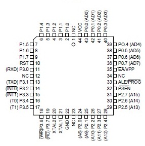
AT89C51

Description

 The AT89C51 is a low-power, high-performance CMOS 8-bit microcomputer with 4Kbytes of Flash programmable and erasable read only memory (PEROM). The device is manufactured using Atmel’s high-density nonvolatile memory technology and is compatible with the industry-standard MCS-51 instruction set and pinout. The on-chip Flash allows the program memory to be reprogrammed in-system or by a conventional nonvolatile memory programmer. By combining a versatile 8-bit CPU with Flash on a monolithic chip, the Atmel AT89C51 is a powerful microcomputer which provides a highly-flexible and cost-effective solution to many embedded control applications.

The AT89C51 provides the following standard features: 4K bytes of Flash, 128 bytes of RAM, 32 I/O lines, two 16-bit timer/counters, a five vector two-level interrupt architecture, a full duplex serial port, on-chip oscillator and clock circuitry. In addition, the AT89C51 is designed with static logic for operation down to zero frequency and supports two software selectable power saving modes. The Idle Mode stops the CPU while allowing the RAM, timer/counters, serial port and interrupt system to continue functioning. The Power-down Mode saves the RAM contents but freezes the oscillator disabling all other chip functions until the next hardware reset.


Features
  • Compatible with MCS-51™ Products
  • 4K Bytes of In-System Reprogrammable Flash Memory
  • Fully Static Operation: 0 Hz to 24 MHz
  • Three-level Program Memory Lock
  • 128 x 8-bit Internal RAM
  • 32 Programmable I/O Lines
  • Two 16-bit Timer/Counters
  • Six Interrupt Sources
  • Programmable Serial Channel
  • Low-power Idle and Power-down Modes
Pinout Diagram


Download Datasheet AT89C51

Sunday, April 21, 2013

LM2576

Description

The LM2576 series of regulators are monolithic integrated circuits that provide all the active functions for a step-down (buck) switching regulator, capable of driving 3A load with excellent line and load regulation. These devices are available in fixed output voltages of 3.3V, 5V, 12V, 15V, and an adjustable output version. Requiring a minimum number of external components, these regulators are simple to use and include internal frequency compensation and a fixed frequency oscillator.

The LM2576 series offers a high-efficiency replacement for popular three-terminal linear regulators. It substantially reduces the size of the heat sink, and in some cases no heat sink is required. A standard series of inductors optimized for use with the LM2576 are available from several different manufacturers. This feature greatly simplifies the design of switch-mode power supplies. Other features include a specified ±4% tolerance on output voltage within specified input voltages and output load conditions, and ±10% on the oscillator frequency. External shutdown is included, featuring 50μA (typical) standby current. The output switch includes cycle-by-cycle current limiting, as well as thermal shutdown for full protection under fault conditions.

Blok Diagram
Download Datasheet LM2576

TDA2030

DESCRIPTION

The TDA2030 is a monolithic integrated circuit in Penta watt® package, intended for use as a low frequency class AB amplifier. Typically it provides 14W output power (d = 0.5%) at 14V/4Ω; at ± 14V or 28V, the guaranteed output power is 12W on a 4Ω load and 8W on a 8Ω (DIN45500).

The TDA2030 provides high output current and has very low harmonic and cross-over distortion. Further the device incorporates an original (and patented) short circuit protection system comprising an arrangement for automatically limiting the dissipated power so as to keep the working point of the output transistors within their safe operating area. A conventional thermal shut-down system is also included.

PRACTICAL CONSIDERATIONS

Printed circuit board
The layout shown in Fig. 1 should be adopted by the designers. If different layouts are used, the
ground points of input 1 and input 2 must be well decoupled from the ground return of the output in
which a high current flows.
 Fig 1

Assembly suggestion
No electrical isolation is needed between the package and the heatsink with single supply voltage configuration.


Application suggestions
The recommended values of the components are those shown on application circuit of fig. 2. Different values can be used. The following table can help the designer.

Fig 2
SHORT CIRCUIT PROTECTION
The TDA2030 has an original circuit which limits the current of the output transistors. Fig. 3 shows that the maximum output current is a function of the collector emitter voltage; hence the output transistors work within their safe operating area. This function can therefore be considered as being peak power limiting rather than simple current limiting. It reduces the possibility that the device gets damaged during an accidental short circuit from AC output to ground.
 Fig 3
THERMAL SHUT-DOWN
The presence of a thermal limiting circuit offers the following advantages:
  1. An overload on the output (even if it is permanent), or an above limit ambient temperature can be easily supported since the Tj cannot be higher than 150°C.
  2. The heatsink can have a smaller factor of safety compared with that of a conventional circuit. There is no possibility of device damage due to high junction temperature. If for any reason, the junction temperature increases up to 150°C, the thermal shut-down simply reduces the power dissipation at the current consumption.
The maximum allowable power dissipation depends upon the size of the external heatsink (i.e. its
thermal resistance).

AT90S2313


Description


The AT90S2313 is a low-power CMOS 8-bit microcontroller based on the AVR RISC architecture. By executing powerful instructions in a single clock cycle, the AT90S2313 achieves throughputs approaching 1 MIPS per MHz allowing the system designer to optimize power consumption versus processing speed.

The AVR core combines a rich instruction set with 32 general purpose working registers. All the 32 registers are directly connected to the Arithmetic Logic Unit (ALU), allowing two independent registers to be accessed in one single instruction executed in one clock cycle. The resulting architecture is more code efficient while achieving through puts up to ten times faster than conventional CISC micro controllers.

The AT90S2313 provides the following features: 2K bytes of In-System Programmable Flash, 128bytes EEPROM, 128 bytes SRAM, 15 general purpose I/O lines, 32 general purpose working registers, flexible Timer/Counters with compare modes, internal and external interrupts, a programmable serial UART, programmable Watchdog Timer with internal Oscillator, an SPI serial port for Flash memory downloading and two software selectable power-saving modes. The Idle mode stops the CPU while allowing the SRAM, Timer/Counters, SPI port and interrupt system to continue functioning. The Power-down mode saves the register contents but freezes the Oscillator, disabling all other chip functions until the next external interrupt or Hardware Reset.

The device is manufactured using Atmel’s high-density non-volatile memory technology. The On-chip In-System Programmable Flash allows the Program memory to be reprogrammed in-system through an SPI serial interface or by a conventional non-volatile memory programmer. By combining an enhanced RISC 8-bit CPU with In-System Programmable Flash on a monolithic chip, the Atmel AT90S2313 is a powerful microcontroller that provides a highly flexible and cost-effective solution to many embedded control applications.

The AT90S2313 AVR is supported with a full suite of program and system development tools including: C compilers, macro assemblers, program debugger/simulators, In-Circuit Emulators and evaluation kits.

Features
  • Utilizes the AVR ® RISC Architecture
  • AVR High Performance and Low Power RISC Architecture
  • 118 Powerful Instructions
  • Most Single Clock Cycle Execution
  • 32 x 8 General Purpose Working Registers
  • Up to 10 MIPS Throughput at 10 MHz
  •  Data and Non-volatile Program Memory
  • 2K Bytes of In-System Programmable Flash Endurance 1,000 Write/Erase Cycles
  • 128 Bytes of SRAM
  • 128 Bytes of In-System Programmable EEPROM Endurance: 100,000 Write/Erase Cycles
  • Programming Lock for Flash Program and EEPROM Data Security
  •  Peripheral Features
  • One 8-bit Timer/Counter with Separate Prescaler 
  • One 16-bit Timer/Counter with Separate Prescaler, Compare, Capture Modes and 8, 9, or 10 bit PWM
  • On-chip Analog Comparator
  • Programmable Watchdog Timer with On-chip Oscillator
  • SPI Serial Interface for In-System Programming 
  • Full Duplex UART
  • Special Micro controller Features
  • Low Power Idle and Power-down Modes
  • External and Internal Interrupt Sources
  • Specifications
  • Low-power, High-speed CMOS Process Technology
  • Fully Static Operation
  • Power Consumption at 4 MHz, 3V, 25°C
  • Active: 2.8 mA
  • Idle Mode: 0.8 mA
  • Power-down Mode: <1 µA
  •  I/O and Packages
  • 15 Programmable I/O Lines
  • 20-pin PDIP and SOIC
  • Operating Voltages
  • 2.7 - 6.0V (AT90S2313-4)
  • 4.0 - 6.0V (AT90S2313-10)
  • Speed Grades
  • 0 - 4 MHz (AT90S2313-4)
  • 0 - 10 MHz (AT90S2313-10)
 Pin Configuration

Download Datasheet AT90S2313