Showing posts with label IC Microcontroller. Show all posts

Monday, June 17, 2013

ATMEGA64

Description

The ATmega64 is a low-power CMOS 8-bit microcontroller based on the AVR enhanced RISC architecture. By executing powerful instructions in a single clock cycle, the ATmega64 achieves throughputs approaching 1 MIPS per MHz, allowing the system designer to optimize power consumption versus processing speed.
The AVR core combines a rich instruction set with 32 general  purpose working registers. All the 32 registers are directly connected to the Arithmetic Logic Unit (ALU), allowing two independent registers to be accessed in one single instruction executed in one clock cycle. The resulting architecture is more code efficient while achieving throughputs up to ten times faster than conventional CISC microcontrollers.

The ATmega64 provides the following features: 64 Kbytes of In-System Programmable Flash with Read-While-Write capabilities, 2 Kbytes EEPROM, 4 Kbytes SRAM, 53 general purpose I/O lines, 32 general purpose working registers, Real Time Counter (RTC), four flexible Timer/Counters with compare modes and PWM, two USARTs, a byte oriented Two-wire Serial Interface, an 8-channel, 10-bit ADC with optional differential input stage with programmable gain, programmable Watchdog Timer with internal  Oscillator, an SPI serial port, IEEE std. 1149.1 compliant JTAG test interface, also used for accessing the On-chip Debug system and programming, and six software selectable power saving modes. The Idle mode stops the CPU while allowing the SRAM, Timer/Counters, SPI port, and interrupt system to continue functioning. The Power-down mode saves the register contents but freezes the Oscillator, disabling all other chip functions until the next interrupt or Hardware Reset. In Power-save mode, the asynchronous timer continues to run, allowing the user to maintain a timer base while the rest of the device is sleeping. The ADC Noise Reduction mode stops the CPU and all I/O modules except asynchronous timer and ADC, to minimize switching noise during ADC conversions. In Standby mode, the crystal/resonator Oscillator is running while the rest of the device is sleeping. This allows very fast start-up combined with low power consumption. In Extended Standby mode, both the main Oscillator and the asynchronous timer continue to run.

Pinout ATMEGA64
Download Datasheet ATMEGA64

Sunday, June 16, 2013

AT89C51

Description

 The AT89C51 is a low-power, high-performance CMOS 8-bit microcomputer with 4Kbytes of Flash programmable and erasable read only memory (PEROM). The device is manufactured using Atmel’s high-density nonvolatile memory technology and is compatible with the industry-standard MCS-51 instruction set and pinout. The on-chip Flash allows the program memory to be reprogrammed in-system or by a conventional nonvolatile memory programmer. By combining a versatile 8-bit CPU with Flash on a monolithic chip, the Atmel AT89C51 is a powerful microcomputer which provides a highly-flexible and cost-effective solution to many embedded control applications.

The AT89C51 provides the following standard features: 4K bytes of Flash, 128 bytes of RAM, 32 I/O lines, two 16-bit timer/counters, a five vector two-level interrupt architecture, a full duplex serial port, on-chip oscillator and clock circuitry. In addition, the AT89C51 is designed with static logic for operation down to zero frequency and supports two software selectable power saving modes. The Idle Mode stops the CPU while allowing the RAM, timer/counters, serial port and interrupt system to continue functioning. The Power-down Mode saves the RAM contents but freezes the oscillator disabling all other chip functions until the next hardware reset.


Features
  • Compatible with MCS-51™ Products
  • 4K Bytes of In-System Reprogrammable Flash Memory
  • Fully Static Operation: 0 Hz to 24 MHz
  • Three-level Program Memory Lock
  • 128 x 8-bit Internal RAM
  • 32 Programmable I/O Lines
  • Two 16-bit Timer/Counters
  • Six Interrupt Sources
  • Programmable Serial Channel
  • Low-power Idle and Power-down Modes
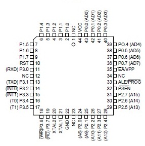
Pinout Diagram


Download Datasheet AT89C51

Sunday, April 21, 2013

AT90S2313


Description


The AT90S2313 is a low-power CMOS 8-bit microcontroller based on the AVR RISC architecture. By executing powerful instructions in a single clock cycle, the AT90S2313 achieves throughputs approaching 1 MIPS per MHz allowing the system designer to optimize power consumption versus processing speed.

The AVR core combines a rich instruction set with 32 general purpose working registers. All the 32 registers are directly connected to the Arithmetic Logic Unit (ALU), allowing two independent registers to be accessed in one single instruction executed in one clock cycle. The resulting architecture is more code efficient while achieving through puts up to ten times faster than conventional CISC micro controllers.

The AT90S2313 provides the following features: 2K bytes of In-System Programmable Flash, 128bytes EEPROM, 128 bytes SRAM, 15 general purpose I/O lines, 32 general purpose working registers, flexible Timer/Counters with compare modes, internal and external interrupts, a programmable serial UART, programmable Watchdog Timer with internal Oscillator, an SPI serial port for Flash memory downloading and two software selectable power-saving modes. The Idle mode stops the CPU while allowing the SRAM, Timer/Counters, SPI port and interrupt system to continue functioning. The Power-down mode saves the register contents but freezes the Oscillator, disabling all other chip functions until the next external interrupt or Hardware Reset.

The device is manufactured using Atmel’s high-density non-volatile memory technology. The On-chip In-System Programmable Flash allows the Program memory to be reprogrammed in-system through an SPI serial interface or by a conventional non-volatile memory programmer. By combining an enhanced RISC 8-bit CPU with In-System Programmable Flash on a monolithic chip, the Atmel AT90S2313 is a powerful microcontroller that provides a highly flexible and cost-effective solution to many embedded control applications.

The AT90S2313 AVR is supported with a full suite of program and system development tools including: C compilers, macro assemblers, program debugger/simulators, In-Circuit Emulators and evaluation kits.

Features
  • Utilizes the AVR ® RISC Architecture
  • AVR High Performance and Low Power RISC Architecture
  • 118 Powerful Instructions
  • Most Single Clock Cycle Execution
  • 32 x 8 General Purpose Working Registers
  • Up to 10 MIPS Throughput at 10 MHz
  •  Data and Non-volatile Program Memory
  • 2K Bytes of In-System Programmable Flash Endurance 1,000 Write/Erase Cycles
  • 128 Bytes of SRAM
  • 128 Bytes of In-System Programmable EEPROM Endurance: 100,000 Write/Erase Cycles
  • Programming Lock for Flash Program and EEPROM Data Security
  •  Peripheral Features
  • One 8-bit Timer/Counter with Separate Prescaler 
  • One 16-bit Timer/Counter with Separate Prescaler, Compare, Capture Modes and 8, 9, or 10 bit PWM
  • On-chip Analog Comparator
  • Programmable Watchdog Timer with On-chip Oscillator
  • SPI Serial Interface for In-System Programming 
  • Full Duplex UART
  • Special Micro controller Features
  • Low Power Idle and Power-down Modes
  • External and Internal Interrupt Sources
  • Specifications
  • Low-power, High-speed CMOS Process Technology
  • Fully Static Operation
  • Power Consumption at 4 MHz, 3V, 25°C
  • Active: 2.8 mA
  • Idle Mode: 0.8 mA
  • Power-down Mode: <1 µA
  •  I/O and Packages
  • 15 Programmable I/O Lines
  • 20-pin PDIP and SOIC
  • Operating Voltages
  • 2.7 - 6.0V (AT90S2313-4)
  • 4.0 - 6.0V (AT90S2313-10)
  • Speed Grades
  • 0 - 4 MHz (AT90S2313-4)
  • 0 - 10 MHz (AT90S2313-10)
 Pin Configuration

Download Datasheet AT90S2313

Friday, December 21, 2012

ATMEGA128

Description

The Atmel® AVR® core combines a rich instruction set with 32 general purpose working registers. All the 32 registers are directly connected to the Arithmetic Logic Unit (ALU), allowing two independent registers to be accessed in one single instruction executed in one clock cycle. The resulting architecture is more code efficient while achieving throughputs up to ten times faster than conventional CISC microcontrollers.

The ATmega128 provides the following features: 128Kbytes of In-System Programmable Flash with Read-While-Write capabilities, 4Kbytes EEPROM, 4Kbytes SRAM, 53 general purpose I/O lines, 32 general purpose working registers, Real Time Counter (RTC), four flexible Timer/Counters with compare modes and PWM, 2 USARTs, a byte oriented Two-wire Serial Interface, an 8-channel, 10-bit ADC with optional differential input stage with programmable gain, programmable Watchdog Timer with Internal Oscillator, an SPI serial port, IEEE std. 1149.1 compliant JTAG test interface, also used for accessing the On-chip Debug system and programming and six software selectable power saving modes. The Idle mode stops the CPU while allowing the SRAM, Timer/Counters, SPI port, and interrupt system to continue functioning. The Power-down mode saves the register contents but freezes the Oscillator, disabling all other chip functions until the next interrupt or Hardware Reset. In Power-save mode, the asynchronous timer continues to run, allowing the user to maintain a timer base while the rest of the device is sleeping.

The ATmega128 is a highly complex microcontroller where the number of I/O locations supersedes the 64 I/O locations reserved in the AVR instruction set. To ensure backward compatibility with the ATmega103, all I/O locations present in ATmega103 have the same location in ATmega128. Most additional I/O locations are added in an Extended I/O space starting from $60 to $FF, (i.e., in the ATmega103 internal RAM space). These locations can be reached by using LD/LDS/LDD and ST/STS/STD instructions only, not by using IN and OUT instructions. The relocation of the internal RAM space may still be a problem for ATmega103 users. Also, the increased number of interrupt vectors might be a problem if the code uses absolute addresses. To solve these problems, an ATmega103 compatibility mode can be selected by programming
the fuse M103C. In this mode, none of the functions in the Extended I/O space are in use, so the internal RAM is located as in ATmega103. Also, the Extended Interrupt vectors are removed.

Features :

  • High-performance, Low-power AVR 8-bit Microcontroller
    • 133 Powerful Instructions - Most Single Clock Cycle Execution 
    • 32 x 8 General Purpose Working Registers + Peripheral Control Resister
    • Up to 16 MIPS Throughput at 16MHz 
    • Fully Static Operation 
    • On-chip 2-cycle Multiplier
  • Non-volatile Program and Data Memories
    • 128k Bytes of In-System Self-Programmable Flash 
    • Optional Boot Code Section with Independent Lock Bits
    • 4K Bytes EEPROM
    • 4K Bytes Internal SRAM
    • Programming Lock for Software Security
    • Up to 64K Bytes Optional External Memory Space 
    • SPI Interface for In-System Programming
  • JTAG Interface
    • Boundary-scan Capabilities According to the JTAG Standard 
    • Extensive On-chip Debug Support 
    • Programming of Flash, EEPROM, Fuses, and Lock Bits through the JTAGS Interface
  • Peripheral Features
    • On-chip Analog Comparator 
    • Programmable Watchdog Timer with Seperate On-chip Oscillator
    • Master/Slave SPI Serial Interface
    • Two 8-bit Timer/Counters with Separate Prescalar, Compare
    • Two Expanded 16-bit Timer/Counters with Seperate Prescaler, Compare and Capture mode
    • Real Time Counter with Separate Oscillator
    • Six PWM Channels with Programmable Resolution from 1 to 16 Bits
    • Dual Programmable Serial USARTs
    • 8-channel, 10-bit ADC
    • Byte-oriented Two-wire Serial Interface
    • Four PWM Channels 
    • Dual Programmable Serial USARTs
  • I/O and Packages
    • 53 Programmable I/O Lines 
    • 64-lead TQFP, and 64-pad MLF
  • Operating Voltages
    • 4.5-5.5V for ATmega128
  • Speed Grades
    • 0-16 MHz for ATmega128
  • Special Microcontroller Features
    • Power-on Reset and Programmable Brown-out Detection 
    • Internal Calibrated RC Oscillator
    • External and Internal Interrupt Sources 
    • Six Sleep Modes: Idle, ADC Noise Reduction, Power-save, Power-down, Standby, and Extended Standby
    • Software selectable Clock Frequence
    • ATmega103 Compatibility Mode Selected by a Fuse
    • Global Pull-up Disable
  •  

Monday, December 17, 2012

ATMEGA32

Description

The Atmel®AVR®AVR core combines a rich instruction set with 32general purpose working registers. All the 32 registers are directly connected to the Arithmetic Logic Unit (ALU), allowing two independent registers to be accessed in one single instruction executed in one clock cycle. The resulting architecture is more code efficient while achieving throughputs up to ten times faster than conventional CISC microcontrollers.

The ATmega32 provides the following features: 32Kbytes of In-System Programmable Flash Program memory with Read-While-Write capabilities, 1024bytes EEPROM, 2Kbyte SRAM, 32 general purpose I/O lines, 32 general purpose working registers, a JTAG interface for Boundaryscan, On-chip Debugging support and programming, three flexible Timer/Counters with compare modes, Internal and External Interrupts, a serial programmable USART, a byte oriented Two-wire Serial Interface, an 8-channel, 10-bit ADC with optional differential input stage with programmable gain (TQFP package only), a programmable Watchdog Timer with Internal Oscillator, an SPI serial port, and six software selectable power saving modes. The Idle mode stops the CPU while allowing the USART, Two-wire interface, A/D Converter, SRAM, Timer/Counters, SPI port, and interrupt system to continue functioning. The Power-down mode saves the register contents but freezes the Oscillator, disabling all other chip functions until the next External Interrupt or Hardware Reset. In Power-save mode, the Asynchronous Timer continues to run, allowing the user to maintain a timer base while the rest of the device is sleeping. The ADC Noise Reduction mode stops the CPU and all I/O modules except Asynchronous Timer and ADC, to minimize switching noise during ADC conversions. In Standby mode, the crystal/resonator Oscillator is running while the rest of the device is sleeping. This allows very fast start-up combined with low-power consumption. In Extended Standby mode, both the main Oscillatorand the Asynchronous Timer continue to run.

Features

  • High-performance, Low-power Atmel®AVR® 8-bit Microcontroller
  • Advanced RISC Architecture
    – 131 Powerful Instructions – Most Single-clock Cycle Execution
    – 32 × 8 General Purpose Working Registers
    – Fully Static Operation
    – Up to 16 MIPS Throughput at 16MHz
    – On-chip 2-cycle Multiplier
  • High Endurance Non-volatile Memory segments
    – 32Kbytes of In-System Self-programmable Flash program memory
    – 1024Bytes EEPROM
    – 2Kbytes Internal SRAM
    – Write/Erase Cycles: 10,000 Flash/100,000 EEPROM
    – Data retention: 20 years at 85°C/100 years at 25°C(1)
    – Optional Boot Code Section with Independent Lock Bits
       In-System Programming by On-chip Boot Program
       True Read-While-Write Operation
    – Programming Lock for Software Security
  • JTAG (IEEE std. 1149.1 Compliant) Interface
    – Boundary-scan Capabilities According to the JTAG Standard
    – Extensive On-chip Debug Support
    – Programming of Flash, EEPROM, Fuses, and Lock Bits through the JTAG Interface
  • Peripheral Features
    – Two 8-bit Timer/Counters with Separate Prescalers and Compare Modes
    – One 16-bit Timer/Counter with Separate Prescaler, Compare Mode, and Capture Mode
    – Real Time Counter with Separate Oscillator
    – Four PWM Channels
    – 8-channel, 10-bit ADC
       8 Single-ended Channels
       7 Differential Channels in TQFP Package Only
       2 Differential Channels with Programmable Gain at 1x, 10x, or 200x
    – Byte-oriented Two-wire Serial Interface
    – Programmable Serial USART
    – Master/Slave SPI Serial Interface
    – Programmable Watchdog Timer with Separate On-chip Oscillator
    – On-chip Analog Comparator
  • Special Microcontroller Features
    – Power-on Reset and Programmable Brown-out Detection
    – Internal Calibrated RC Oscillator
    – External and Internal Interrupt Sources
    – Six Sleep Modes: Idle, ADC Noise Reduction, Power-save, Power-down, Standby
       and Extended Standby
  • I/O and Packages
    – 32 Programmable I/O Lines
    – 40-pin PDIP, 44-lead TQFP, and 44-pad QFN/MLF
  • Operating Voltages
    – 2.7V - 5.5V for ATmega32L
    – 4.5V - 5.5V for ATmega32
  • Speed Grades
    – 0 - 8MHz for ATmega32L
    – 0 - 16MHz for ATmega32
  • Power Consumption at 1MHz, 3V, 25°C
    – Active: 1.1mA
    – Idle Mode: 0.35mA
    – Power-down Mode: < 1μA

Pinout Diagram

Download Datasheet ATMEGA32

ATMEGA16


 Description

The ATmega16 is a low-power CMOS 8-bit microcontroller based on the AVR enhanced RISC architecture. By executing powerful instructions in a single clock cycle, the ATmega16 achieves throughputs approaching 1 MIPS per MHz allowing the system designer to optimize power consumption versus processing speed.

The ATmega16 provides the following features: 16 Kbytes of In-System Programmable Flash Program memory with Read-While-Write capabilities, 512 bytes EEPROM, 1 Kbyte SRAM, 32 general purpose I/O lines, 32 general purpose working registers, a JTAG interface for Boundaryscan, On-chip Debugging support and programming, three flexible Timer/Counters with compare modes, Internal and External Interrupts, a serial programmable USART, a byte oriented Two-wire Serial Interface, an 8-channel, 10-bit ADC with optional differential input stage with programmable gain (TQFP package only), a programmable Watchdog Timer with Internal Oscillator, an SPI serial port, and six software selectable power saving modes. The Idle mode stops the CPU while allowing the USART, Two-wire interface, A/D Converter, SRAM, Timer/Counters, SPI port, and interrupt system to continue functioning. The Power-down mode saves the register contents but freezes the Oscillator, disabling all other chip functions until the next External Interrupt or Hardware Reset. In Power-save mode, the Asynchronous Timer continues to run, allowing the user to maintain a timer base while the rest of the device is sleeping. The ADC Noise Reduction mode stops the CPU and all I/O modules except Asynchronous Timer and ADC, to minimize switching noise during ADC conversions. In Standby mode, the crystal/resonator Oscillator is running while the rest of the device is sleeping. This allows very fast start-up combined with low-power consumption. In Extended Standby mode, both the main Oscillator and the Asynchronous Timer continue to run.

Features:

  • High-performance, Low-power Atmel® AVR® 8-bit Microcontroller
  • Advanced RISC Architecture
    – 131 Powerful Instructions – Most Single-clock Cycle Execution
    – 32 x 8 General Purpose Working Registers
    – Fully Static Operation
    – Up to 16 MIPS Throughput at 16 MHz
    – On-chip 2-cycle Multiplier
  • High Endurance Non-volatile Memory segments
    – 16 Kbytes of In-System Self-programmable Flash program memory
    – 512 Bytes EEPROM
    – 1 Kbyte Internal SRAM
    – Write/Erase Cycles: 10,000 Flash/100,000 EEPROM
    – Data retention: 20 years at 85°C/100 years at 25°C(1)
    – Optional Boot Code Section with Independent Lock Bits
       In-System Programming by On-chip Boot Program
       True Read-While-Write Operation
    – Programming Lock for Software Security
  • JTAG (IEEE std. 1149.1 Compliant) Interface
    – Boundary-scan Capabilities According to the JTAG Standard
    – Extensive On-chip Debug Support
    – Programming of Flash, EEPROM, Fuses, and Lock Bits through the JTAG Interface]
  • Peripheral Features
    – Two 8-bit Timer/Counters with Separate Prescalers and Compare Modes
    – One 16-bit Timer/Counter with Separate Prescaler, Compare Mode, and Capture Mode
    – Real Time Counter with Separate Oscillator
    – Four PWM Channels
    – 8-channel, 10-bit ADC
       8 Single-ended Channels
       7 Differential Channels in TQFP Package Only
       2 Differential Channels with Programmable Gain at 1x, 10x, or 200x
    – Byte-oriented Two-wire Serial Interface
    – Programmable Serial USART
    – Master/Slave SPI Serial Interface
    – Programmable Watchdog Timer with Separate On-chip Oscillator
    – On-chip Analog Comparator
  • Special Microcontroller Features
    – Power-on Reset and Programmable Brown-out Detection
    – Internal Calibrated RC Oscillator
    – External and Internal Interrupt Sources
    – Six Sleep Modes: Idle, ADC Noise Reduction, Power-save, Power-down, Standby
       and Extended Standby
  • I/O and Packages
    – 32 Programmable I/O Lines
    – 40-pin PDIP, 44-lead TQFP, and 44-pad QFN/MLF
  • Operating Voltages
    – 2.7V - 5.5V for ATmega16L
    – 4.5V - 5.5V for ATmega16
  • Speed Grades
    – 0 - 8 MHz for ATmega16L
    – 0 - 16 MHz for ATmega16
  • Power Consumption @ 1 MHz, 3V, and 25°C for ATmega16L
    – Active: 1.1 mA
    – Idle Mode: 0.35 mA
    – Power-down Mode: < 1 μA

Pinout Diagram

ATMEGA168


 Description


The Atmel ATmega48/88/168 is a low-power CMOS 8-bit microcontroller based on the AVR enhanced RISC architecture. By executing powerful instructions in a single clock cycle, the ATmega48/88/168 achieves throughputs approaching 1 MIPS per MHz allowing the system designer to optimize power consumption versus processing speed.

The Atmel ATmega48/88/168 provides the following features: 4K/8K/16K bytes of In-System Programmable Flash with Read-While-Write capabilities, 256/512/512 bytes EEPROM, 512/1K/1K bytes SRAM, 23 general purpose I/O lines, 32 general purpose working registers, three flexible Timer/Counters with compare modes, internal and external interrupts, a serial programmable USART, a byte-oriented 2-wire Serial Interface, an SPI serial port, a 6-channel 10-bit ADC (8 channels in TQFP and QFN/MLF packages), a programmable Watchdog Timer with internal Oscillator, and five software selectable power saving modes. The Idle mode stops the CPU while allowing the SRAM, Timer/Counters, USART, 2-wire Serial Interface, SPI port, and interrupt system to continue functioning. The Power-down mode saves the register contents but freezes the Oscillator, disabling all other chip functions until the next interrupt or hardware reset. In Power-save mode, the asynchronous timer continues to run, allowing the user to maintain a timer base while the rest of the device is sleeping. The ADC Noise Reduction mode stops the CPU and all I/O modules except asynchronous timer and ADC, to minimize switching noise during ADC conversions. In Standby mode, the crystal/resonator Oscillator is running while the rest of the device is sleeping. This allows very fast start-up combined with low power consumption.

Features :

  • High performance, low power Atmel® AVR® 8-bit microcontroller
  • Advanced RISC architecture
    – 131 powerful instructions – most single clock cycle execution
    – 32 × 8 general purpose working registers
    – Fully static operation
    – Up to 20 MIPS throughput at 20MHz
    – On-chip 2-cycle multiplier
  • High endurance non-volatile memory segments
    – 4/8/16 Kbytes of in-system self-programmable flash program memory
    – 256/512/512 bytes EEPROM
    – 512/1K/1Kbytes internal SRAM
    – Write/erase cyles: 10,000 flash/100,000 EEPROM
    – Data retention: 20 years at 85°C/100 years at 25°C()
    – Optional boot code section with independent lock bits
          In-system programming by on-chip boot program
          True read-while-write operation
    – Programming lock for software security
  • QTouch® library support
    – Capacitive touch buttons, sliders and wheels
    – QTouch and QMatrix acquisition
    – Up to 64 sense channels
  • Peripheral features
    – Two 8-bit timer/counters with separate prescaler and compare mode
    – One 16-bit timer/counter with separate prescaler, compare mode, and capture mode
    – Real time counter with separate oscillator
    – Six PWM channels
    – 8-channel 10-bit ADC in TQFP and QFN/MLF package
    – 6-channel 10-bit ADC in PDIP Package
    – Programmable serial USART
    – Master/slave SPI serial interface
    – Byte-oriented 2-wire serial interface (Philips I2C compatible)
    – Programmable watchdog timer with separate on-chip oscillator
    – On-chip analog comparator
    – Interrupt and wake-up on pin change
  • Special microcontroller features
    – DebugWIRE on-chip debug system
    – Power-on reset and programmable brown-out detection
    – Internal calibrated oscillator
    – External and internal interrupt sources
    – Five sleep modes: Idle, ADC noise reduction, power-save, power-down, and standby
  • I/O and packages
    – 23 programmable I/O lines
    – 28-pin PDIP, 32-lead TQFP, 28-pad QFN/MLF and 32-pad QFN/MLF
  • Operating voltage:
    – 1.8V - 5.5V for Atmel ATmega48V/88V/168V
    – 2.7V - 5.5V for Atmel ATmega48/88/168
  • Temperature range:
    – -40°C to 85°C
  • Speed grade:
    – ATmega48V/88V/168V: 0 - 4MHz @ 1.8V - 5.5V, 0 - 10MHz @ 2.7V - 5.5V
    – ATmega48/88/168: 0 - 10MHz @ 2.7V - 5.5V, 0 - 20MHz @ 4.5V - 5.5V
  • Low power consumption
    – Active mode:
       250μA at 1MHz, 1.8V
       15μA at 32kHz, 1.8V (including oscillator)
    – Power-down mode:
       0.1μA at 1.8V 
     

Pinout Diagram


 Download Datasheet ATMEGA168

ATMEGA8

 Description


The Atmel®AVR® ATmega8A is a low-power CMOS 8-bit microcontroller based on the AVR RISC architecture. By executing powerful instructions in a single clock cycle, the ATmega8A achieves throughputs approaching 1 MIPS per MHz, allowing the system designer to optimize power consumption versus processing speed.

The Atmel®AVR® AVR core combines a rich instruction set with 32 general purpose working registers. All the 32 registers are directly connected to the Arithmetic Logic Unit (ALU), allowing two independent registers to be accessed in one single instruction executed in one clock cycle. The resulting architecture is more code efficient while achieving throughputs up to ten times faster than conventional CISC microcontrollers.

The ATmega8A provides the following features: 8K bytes of In-System Programmable Flash with Read-While-Write capabilities, 512 bytes of EEPROM, 1K byte of SRAM, 23 general purpose I/O lines, 32 general purpose working registers, three flexible Timer/Counters with compare modes, internal and external interrupts, a serial programmable USART, a byte oriented Two-wire Serial Interface, a 6-channel ADC (eight channels in TQFP and QFN/MLF packages) with 10-bit accuracy, a programmable Watchdog Timer with Internal Oscillator, an SPI serial port, and five software selectable power saving modes. The Idle mode stops the CPU while allowing the SRAM, Timer/Counters, SPI port, and interrupt system to continue functioning. The Power-down mode saves the register contents but freezes the Oscillator, disabling all other chip functions until the next Interrupt or Hardware Reset. In Power-save mode, the asynchronous timer continues to run, allowing the user to maintain a timer base while the rest of the device is sleeping. The ADC Noise Reduction mode stops the CPU and all I/O modules except asynchronous timer and ADC, to minimize switching noise during ADC conversions. In Standby mode, the crystal/resonator Oscillator is running while the rest of the device is sleeping. This allows very fast start-up combined with low-power consumption.

Features :

  •  High-performance, Low-power Atmel®AVR® 8-bit Microcontroller
  • Advanced RISC Architecture
    – 130 Powerful Instructions – Most Single-clock Cycle Execution
    – 32 x 8 General Purpose Working Registers
    – Fully Static Operation
    – Up to 16MIPS Throughput at 16MHz
    – On-chip 2-cycle Multiplier
  • High Endurance Non-volatile Memory segments
    – 8KBytes of In-System Self-programmable Flash program memory
    – 512Bytes EEPROM
    – 1KByte Internal SRAM
    – Write/Erase Cycles: 10,000 Flash/100,000 EEPROM
    – Data retention: 20 years at 85°C/100 years at 25°C(1)
    – Optional Boot Code Section with Independent Lock Bits
       • In-System Programming by On-chip Boot Program
       • True Read-While-Write Operation
    – Programming Lock for Software Security
  • Peripheral Features
    – Two 8-bit Timer/Counters with Separate Prescaler, one Compare Mode
    – One 16-bit Timer/Counter with Separate Prescaler, Compare Mode, and Capture
    Mode
    – Real Time Counter with Separate Oscillator
    – Three PWM Channels
    – 8-channel ADC in TQFP and QFN/MLF package
        • Eight Channels 10-bit Accuracy
    – 6-channel ADC in PDIP package
        • Six Channels 10-bit Accuracy
    – Byte-oriented Two-wire Serial Interface
    – Programmable Serial USART
    – Master/Slave SPI Serial Interface
    – Programmable Watchdog Timer with Separate On-chip Oscillator
    – On-chip Analog Comparator
  • Special Microcontroller Features
    – Power-on Reset and Programmable Brown-out Detection
    – Internal Calibrated RC Oscillator
    – External and Internal Interrupt Sources
    – Five Sleep Modes: Idle, ADC Noise Reduction, Power-save, Power-down, and Standby
  • I/O and Packages
    – 23 Programmable I/O Lines
    – 28-lead PDIP, 32-lead TQFP, and 32-pad QFN/MLF
  • Operating Voltages
    – 2.7 - 5.5V
    – 0 - 16MHz
  • Power Consumption at 4MHz, 3V, 25°C
    – Active: 3.6mA
    – Idle Mode: 1.0mA
    – Power-down Mode: 0.5μA

Pinout Diagram

Download Datasheet ATMEGA8

ATMEGA8535L

Description


The high-performance, low-power Atmel 8-bit AVR RISC-based microcontroller combines 8KB of programmable flash memory, 544B SRAM, 512B EEPROM, and an 8-channel 10-bit A/D converter. The device supports throughput of 16 MIPS at 16MHz and operates between 4.5-5.5 volts. By executing instructions in a single clock cycle, the device achieves throughputs approaching 1 MIPS per MHz, balancing power consumption and processing speed.

The AVR core combines a rich instruction set with 32 general purpose working registers. All 32 registers are directly connected to the Arithmetic Logic Unit (ALU), allowing two independent registers to be accessed in one single instruction executed in one clock cycle. The resulting architecture is more code efficient while achieving throughputs up to ten times faster than conventional CISC microcontrollers.

The ATmega8535 provides the following features: 8K bytes of In-System Programmable Flash with Read-While-Write capabilities, 512 bytes EEPROM, 512 bytes SRAM, 32 general purpose I/O lines, 32general purpose working registers, three flexible Timer/Counters with compare modes, internal and external interrupts, a serial programmable USART, a byte oriented Two-wire Serial Interface, an 8-channel, 10-bit ADC with optional differential input stage with programmable gain in TQFP package, a programmable Watchdog Timer with Internal Oscillator, an SPI serial port, and six software selectable power saving modes. The Idle mode stops the CPU while allowing the SRAM, Timer/Counters, SPI port, and interrupt system to continue functioning. The Power-down mode saves the register contents but freezes the Oscillator, disabling all other chip functions until the next interrupt or Hardware Reset. In Power-save mode, the asynchronous timer continues to run, allowing the user to maintain a timer base while the rest of the device is sleeping. The ADC Noise Reduction mode stops the CPU and all I/O modules except asynchronous timer and ADC, to minimize switching noise during ADC conversions. In Standby mode, the crystal/resonator Oscillator is running while the rest of the device is sleeping. This allows very fast start-up combined with low-power consumption. In Extended Standby mode, both the main Oscillator and the asynchronous timer continue to run.

Features :

  • High-performance, Low-power AVR® 8-bit Microcontroller
  • Advanced RISC Architecture
    – 130 Powerful Instructions – Most Single Clock Cycle Execution
    – 32 x 8 General Purpose Working Registers
    – Fully Static Operation
    – Up to 16 MIPS Throughput at 16 MHz
    – On-chip 2-cycle Multiplier
  • Nonvolatile Program and Data Memories
    – 8K Bytes of In-System Self-Programmable Flash
       Endurance: 10,000 Write/Erase Cycles
    – Optional Boot Code Section with Independent Lock Bits In-System Programming by On-chip Boot Program True Read-While-Write Operation
    – 512 Bytes EEPROM
       Endurance: 100,000 Write/Erase Cycles
    – 512 Bytes Internal SRAM
    – Programming Lock for Software Security
  • Peripheral Features
    – Two 8-bit Timer/Counters with Separate Prescalers and Compare Modes
    – One 16-bit Timer/Counter with Separate Prescaler, Compare Mode, and Capture Mode
    – Real Time Counter with Separate Oscillator
    – Four PWM Channels
    – 8-channel, 10-bit ADC
    8 Single-ended Channels
    7 Differential Channels for TQFP Package Only
    2 Differential Channels with Programmable Gain at 1x, 10x, or 200x for TQFP
    Package Only
    – Byte-oriented Two-wire Serial Interface
    – Programmable Serial USART
    – Master/Slave SPI Serial Interface
    – Programmable Watchdog Timer with Separate On-chip Oscillator
    – On-chip Analog Comparator
  • Special Microcontroller Features
    – Power-on Reset and Programmable Brown-out Detection
    – Internal Calibrated RC Oscillator
    – External and Internal Interrupt Sources
    – Six Sleep Modes: Idle, ADC Noise Reduction, Power-save, Power-down, Standby
       and Extended Standby
  • I/O and Packages
    – 32 Programmable I/O Lines
    – 40-pin PDIP, 44-lead TQFP, 44-lead PLCC, and 44-pad QFN/MLF
  • Operating Voltages
    – 2.7 - 5.5V for ATmega8535L
    – 4.5 - 5.5V for ATmega8535
  • Speed Grades
    – 0 - 8 MHz for ATmega8535L
    – 0 - 16 MHz for ATmega8535

Pinout Diagram

Download Datasheet ATMEGA8535

ATMEGA8515


Description


The ATmega8515 is a low-power CMOS 8-bit microcontroller based on the AVR enhanced RISC architecture. By executing powerful instructions in a single clock cycle, the ATmega8515 achieves throughputs approaching 1 MIPS per MHz allowing the system designer to optimize power consumption versus processing speed.

The ATmega8515 provides the following features: 8K bytes of In-System Programmable Flash with Read-While-Write capabilities, 512 bytes EEPROM, 512 bytes SRAM, an External memory interface, 35 general purpose I/O lines, 32 general purpose working registers, two flexible Timer/Counters with compare modes, Internal and External interrupts, a Serial Programmable USART, a programmable Watchdog Timer with internal Oscillator, a SPI serial port, and three software selectable power saving modes. The Idle mode stops the CPU while allowing the SRAM, Timer/Counters, SPI port, and Interrupt system to continue functioning. The Power-down mode saves the Register contents but freezes the Oscillator, disabling all other chip functions until the next interrupt or hardware reset. In Standby mode, the crystal/resonator Oscillator is running while the rest of the device is sleeping. This allows very fast start-up combined with low-power
consumption.

The device is manufactured using Atmel’s high density nonvolatile memory technology. The On-chip ISP Flash allows the Program memory to be reprogrammed In-System through an SPI serial interface, by a conventional nonvolatile memory programmer, or by an On-chip Boot program running on the AVR core. The boot program can use any interface to download the application program in the Application Flash memory. Software in the Boot Flash section will continue to run while the Application Flash section is updated, providing true Read-While-Write operation. By combining an 8-bit RISC CPU with In-System Self-programmable Flash on a monolithic chip, the Atmel ATmega8515 is a powerful microcontroller that provides a highly flexible and cost effective solution to many embedded control applications.

Features :

  • High-performance, Low-power AVR® 8-bit Microcontroller
  • RISC Architecture
    – 130 Powerful Instructions – Most Single Clock Cycle Execution
    – 32 x 8 General Purpose Working Registers
    – Fully Static Operation
    – Up to 16 MIPS Throughput at 16 MHz
    – On-chip 2-cycle Multiplier
  • Nonvolatile Program and Data Memories
    – 8K Bytes of In-System Self-programmable Flash
       Endurance: 10,000 Write/Erase Cycles
    – Optional Boot Code Section with Independent Lock bits
       In-System Programming by On-chip Boot Program
       True Read-While-Write Operation
    – 512 Bytes EEPROM
       Endurance: 100,000 Write/Erase Cycles
    – 512 Bytes Internal SRAM
    – Up to 64K Bytes Optional External Memory Space
    – Programming Lock for Software Security
  • Peripheral Features
    – One 8-bit Timer/Counter with Separate Prescaler and Compare Mode
    – One 16-bit Timer/Counter with Separate Prescaler, Compare Mode, and Capture Mode
    – Three PWM Channels
    – Programmable Serial USART
    – Master/Slave SPI Serial Interface
    – Programmable Watchdog Timer with Separate On-chip Oscillator
    – On-chip Analog Comparator
  • Special Microcontroller Features
    – Power-on Reset and Programmable Brown-out Detection
    – Internal Calibrated RC Oscillator
    – External and Internal Interrupt Sources
    – Three Sleep Modes: Idle, Power-down and Standby
  • I/O and Packages
    – 35 Programmable I/O Lines
    – 40-pin PDIP, 44-lead TQFP, 44-lead PLCC, and 44-pad QFN/MLF
  • Operating Voltages
    – 2.7 - 5.5V for ATmega8515L
    – 4.5 - 5.5V for ATmega8515
  • Speed Grades
    – 0 - 8 MHz for ATmega8515L
    – 0 - 16 MHz for ATmega8515

Pinout Diagram


Download Datasheet ATMEGA8515


AT90S1200

Description

The AT90S1200 is a low-power CMOS 8-bit microcontroller based on the AVR RISC architecture. By executing powerful instructions in a single clock cycle, the AT90S1200 achieves throughputs approaching 1 MIPS per MHz allowing the system designer to optimize power consumption versus processing speed.

The AVR core combines a rich instruction set with the 32 general purpose working registers. All the 32 registers are directly connected to the Arithmetic Logic Unit (ALU), allowing two independent registers to be accessed in one single instruction executed in one clock cycle. The resulting architecture is more code efficient while achieving throughputs up to ten times faster than conventional CISC microcontrollers.

Features:

  • Utilizes the AVR® RISC Architecture
  • AVR – High-performance and Low-power RISC Architecture
    – 89 Powerful Instructions – Most Single Clock Cycle Execution
    – 32 x 8 General Purpose Working Registers
    – Up to 12 MIPS Throughput at 12 MHz
  • Data and Non-volatile Program Memory
    – 1K Byte of In-System Programmable Flash
       Endurance: 1,000 Write/Erase Cycles
    – 64 Bytes of In-System Programmable EEPROM
       Endurance: 100,000 Write/Erase Cycles
    – Programming Lock for Flash Program and EEPROM Data Security
  • Peripheral Features
    – One 8-bit Timer/Counter with Separate Prescaler
    – On-chip Analog Comparator
    – Programmable Watchdog Timer with On-chip Oscillator
    – SPI Serial Interface for In-System Programming
  • Special Microcontroller Features
    – Low-power Idle and Power-down Modes
    – External and Internal Interrupt Sources
    – Selectable On-chip RC Oscillator for Zero External Components
  • Specifications
    – Low-power, High-speed CMOS Process Technology
    – Fully Static Operation
  • Power Consumption at 4 MHz, 3V, 25°C
    – Active: 2.0 mA
    – Idle Mode: 0.4 mA
    – Power-down Mode: <1 μA
  • I/O and Packages
    – 15 Programmable I/O Lines
    – 20-pin PDIP, SOIC and SSOP
  • Operating Voltages
    – 2.7 - 6.0V (AT90S1200-4)
    – 4.0 - 6.0V (AT90S1200-12)
  • Speed Grades
    – 0 - 4 MHz, (AT90S1200-4)
    – 0 - 12 MHz, (AT90S1200-12)

Architectural Overview

The fast-access register file concept contains 32 x 8-bit general purpose working registers with a single clock cycle access time. This means that during one single clock cycle, one ALU (Arithmetic Logic Unit) operation is executed. Two operands are output from the register file, the operation is executed, and the result is stored back in the register file – in one clock cycle.
The ALU supports arithmetic and logic functions between registers or between a constant and a register. Single register operations are also executed in the ALU. The AVR uses a Harvard architecture concept – with separate memories and buses for program and data memories. The program memory is accessed with a 2-stage pipeline. While one instruction is being executed, the next instruction is pre-fetched from the program memory.
This concept enables instructions to be executed in every clock cycle. The program memory is In-System Programmable Flash memory. With the relative jump and relative call instructions, the whole 512 address space is directly accessed. All AVR instructions have a single 16-bit word format, meaning that every program memory address contains a single 16-bit instruction.
During interrupts and subroutine calls, the return address Program Counter (PC) is stored on the stack. The stack is a 3-level-deep hardware stack dedicated for subroutines and interrupts.
The I/O memory space contains 64 addresses for CPU peripheral functions such as Control Registers, Timer/Counters, A/D Converters and other I/O functions. The memory spaces in the AVR architecture are all linear and regular memory maps. A flexible interrupt module has its control registers in the I/O space with an additional global interrupt enable bit in the status register. All the different interrupts have a separate
interrupt vector in the interrupt vector table at the beginning of the program memory. The different interrupts have priority in accordance with their interrupt vector position. The lower the interrupt vector address, the higher the priority.

Pinout Diagram

Download Datasheet AT90S1200

AT90S8515

Description


The AT90S8515 is a low-power CMOS 8-bit microcontroller based on the AVR ® enhanced RISC architecture. By executing powerful instructions in a single clock cycle, the AT90S8515 achieves throughputs approaching 1 MIPS per MHz allowing the system designer to optimize power consumption versus processing speed. The AVR core combines a rich instruction set with 32 general purpose working registers. All the 32 registers are directly connected to the Arithmetic Logic Unit (ALU), allowing two independent registers to be accessed in one single instruction executed in one clock cycle. The resulting architecture is more code efficient while achieving throughputs up to ten times faster than conventional CISC microcontrollers.

The device is manufactured using Atmel’s high density non-volatile memory technology. The on-chip in-system programmable Flash allows the program memory to be reprogrammed in-system through an SPI serial interface or by a conventional nonvolatile memory programmer. By combining an enhanced RISC 8-bit CPU with In-System Programmable Flash on a monolithic chip, the Atmel AT90S8515 is a powerful microcontroller that provides a highly flexible and cost effective solution to many embedded control applications.

Architectural Overview

The fast-access register file concept contains 32 x 8-bit general purpose working registers with a single clock cycle access time. This means that during one single clock cycle, one ALU (Arithmetic Logic Unit) operation is executed. Two operands are output from the register file, the operation is executed, and the result is stored back in the register file - in one clock cycle. Six of the 32 registers can be used as three 16-bits indirect address register pointers for Data Space addressing - enabling efficient address calculations. One of the three address pointers is also used as the address pointer for the constant table look up function. These added function registers are the 16-bits X-register, Y-register and Z-register.
The ALU supports arithmetic and logic functions between registers or between a constant and a register. Single register operations are also executed in the ALU. In addition to the register operation, the conventional memory addressing modes can be used on the register file as well. This is enabled by the fact that the register file is assigned the 32 lowermost Data Space addresses ($00 - $1F), allowing them to be accessed as though they were ordinary memory locations. The I/O memory space contains 64 addresses for CPU peripheral functions as Control Registers, Timer/Counters, A/D-converters, and other I/O functions.

The I/O Memory can be accessed directly, or as the Data Space locations following those of the register file, $20 - $5F. The AVR uses a Harvard architecture concept - with separate memories and buses for program and data. The program memory is executed with a two stage pipeline. While one instruction is being executed, the next instruction is pre-fetched from the program memory. This concept enables instructions to be executed in every clock cycle. The program memory is in-system programmable Flash memory. With the relative jump and call instructions, the whole 4K address space is directly accessed. Most AVR instructions
have a single 16-bit word format. Every program memory address contains a 16- or 32-bit instruction. During interrupts and subroutine calls, the return address program counter (PC) is stored on the stack. The stack is effectively allocated in the general data SRAM, and consequently the stack size is only limited by the total SRAM size and the usage of the SRAM. All user programs must initial size the SP in the reset routine  (before subroutines or interrupts are executed). The 16-bit stack pointer SP is read/write accessible in the I/O space. The 512 bytes data SRAM can be easily accessed through the five different addressing modes supported in the AVR architecture. The memory spaces in the AVR architecture are all linear and regular memory maps. A flexible interrupt module has its control registers in the I/O space with an additional global interrupt enable bit in the status register. All the different interrupts have a separate interrupt vector in the interrupt vector table at the beginning of the program memory. The different interrupts have priority in accordance with their interrupt vector position. The lower the interrupt vector address the higher the priority.


Pinout Diagram AT90S8515


Download Datasheet AT90S8515